
Sub-THz Hardware IC Technologies: Unlocking the Future of High-Speed Wireless

Sub-THz Hardware IC Technologies: Shaping the Future of High-Speed Wireless
The telecommunications sector is stepping into a new era where Sub-THz frequencies (100–500 GHz) are set to be crucial for meeting the ultra-high-speed, low-latency, and high-capacity demands of 6G. Moving from GHz to Sub-THz opens up exciting opportunities for incredible wireless performance, but it also brings along some serious hurdles in hardware design, signal propagation, and integration.
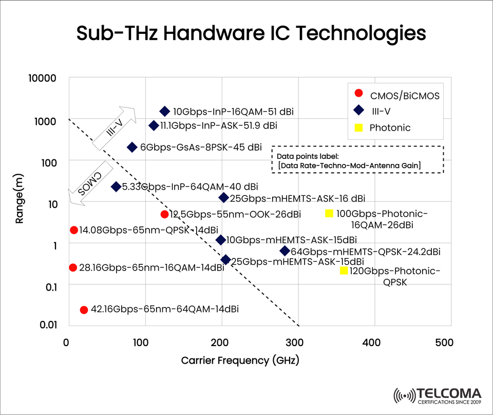
The chart above gives a quick look at Sub-THz Hardware IC Technologies, comparing CMOS/BiCMOS, III-V semiconductors, and Photonic technologies based on carrier frequencies, range, data rates, modulation schemes, and antenna gains. This thorough breakdown helps telecom experts and researchers see how these technologies measure up as we push toward the next generation of wireless systems.
Why Sub-THz Frequencies Matter for 6G
Massive data speeds: The Sub-THz spectrum allows for tens to hundreds of gigabits per second (Gbps)—vital for things like holographic communication, AR/VR, and creating digital twins.
Low latency: Achieving near real-time responses is crucial for autonomous systems and mission-critical IoT applications.
Spectrum availability: With traditional microwave bands getting crowded, the Sub-THz range provides broader bandwidths.
Future-proofing: 5G relies heavily on mmWave, but 6G will move up to Sub-THz to meet the needs of smart cities, AI-driven networks, and immersive experiences.
Key Sub-THz Hardware IC Technologies
The three key players in this space are:
- CMOS/BiCMOS (Red Circles in Chart)
Benefits: * Cost-effective for mass production. * Works well with existing digital/analog circuits. * Highly scalable for consumer devices.
Drawbacks: * Limited output power. * Higher noise and losses at Sub-THz frequencies.
Example from the chart: * 42.16 Gbps at 65nm, 64QAM with 14dBi antenna gain. * Functions below 200 GHz, but only good for short-range (<2 m) applications.
CMOS is great for indoor high-data-rate uses, like wireless VR headsets or short-range chip-to-chip communication.
- III-V Semiconductors (Blue Diamonds in Chart)
This category includes InP (Indium Phosphide), GaAs (Gallium Arsenide), and mHEMTs (Metamorphic High Electron Mobility Transistors).
Advantages: * High electron mobility leads to better performance at higher frequencies. * Can support longer ranges (10 m – 1 km). * Better power handling and efficiency.
Limitations: * More expensive to produce. * Challenges with integration on CMOS platforms.
Examples from the chart: * 10 Gbps InP 16QAM at 51 dBi gain → ~1 km range. * 25 Gbps mHEMT ASK at 16 dBi → mid-range performance. * 64 Gbps mHEMT QPSK at 24.2 dBi → nearing photonic-level data rates.
III-V technologies strike a nice balance between data rate and range, making them fit for wireless backhaul, satellite communications, and outdoor 6G infrastructure.
- Photonic Technologies (Yellow Squares in Chart)
Pros: * Super high data rates — up to 120 Gbps according to the chart. * Perfect for optical-to-wireless convergence, which is essential for seamless integration with fiber-optic networks. * Lots of bandwidth available.
Cons: * Still mostly in the research phase; integration challenges remain. * Needs to tackle cost and power efficiency issues.
Chart examples: * 100 Gbps using 16QAM modulation at 26 dBi gain. * 120 Gbps with QPSK modulation.
Photonics delivers future-ready solutions for ultra-high-capacity links, making it ideal for data centers, inter-satellite communications, and 6G core networks.
Range vs. Frequency Trade-Off
Looking at the chart, a clear trend pops up:
CMOS shines in short-range, low-to-mid frequency Sub-THz applications (<200 GHz, <2 m).
III-V semiconductors extend into longer ranges (up to 1 km) while balancing throughput and antenna gain.
Photonics excels at extremely high data throughput (>100 Gbps), though it has shorter ranges due to physical constraints.
This balance suggests that 6G networks will likely need a hybrid approach, using different hardware ICs based on specific use cases:
Indoor → CMOS.
Outdoor wireless backhaul → III-V.
Core + interconnect → Photonics.
Modulation Schemes and Antenna Gain
The chart also shows various modulation formats such as QPSK, ASK, 8PSK, 16QAM, and 64QAM.
Higher-order modulation (64QAM): * Delivers better spectral efficiency. * Needs a higher SNR (Signal-to-Noise Ratio). * For example: CMOS achieving 42.16 Gbps with 64QAM.
Lower-order modulation (QPSK, ASK): * More resilient against noise. * Works better for longer distances. * For instance: mHEMTs using QPSK at 64 Gbps.
Antenna gain also plays a key role:
Higher gains (40–50 dBi) are necessary for long-distance Sub-THz links.
Lower gains (~14 dBi) work for short-range, high-throughput connections.
Comparative Snapshot
Here’s a quick summary based on the chart:
Technology Range Data Rate (Gbps)Frequency (GHz)Example Use Case CMOS/BiCMOS<2 m12–42<200Indoor short-range links, chip-to-chip commsIII-V10 m – 1 km6–64100–300Wireless backhaul, satellite communicationsPhotonics~10 m100–120>300Data centers, inter-satellite links
Implications for 6G Networks
The rise of Sub-THz hardware IC technologies will change the game for how future wireless systems come together:
Diverse hardware ecosystems: No single tech will rule; a mix is needed for coverage, capacity, and cost-effectiveness.
Beamforming & high-gain antennas: Essential for battling path loss at Sub-THz bands.
Bringing optics and wireless together: Photonics aids in integrating with fiber infrastructure.
Standardization initiatives: Groups like 3GPP and IEEE are pushing Sub-THz into pre-6G research.
🚀 Sub-THz Hardware IC Technologies: The Key to 6G Development
As we move forward with 6G technology, Sub-THz frequencies (100–500 GHz) are shaping up to be essential for super-fast, low-latency wireless systems. But harnessing these capabilities hinges on utilizing the right hardware IC technologies.
🔎 A recent look at CMOS/BiCMOS, III-V semiconductors, and Photonic solutions reveals how each stacks up in terms of carrier frequency, range, data rates, and antenna gains:
📌 CMOS/BiCMOS
✅ Affordable, scalable, and a great fit for consumer devices.
❌ Limited range (<2 m) and lower output power.
Example: 42.16 Gbps (64QAM, 14dBi) at frequencies under 200 GHz.
Best for: Short-distance indoor applications (think VR/AR or chip-to-chip connections).
📌 III-V Semiconductors (InP, GaAs, mHEMTs)
✅ Great for longer ranges (10 m – 1 km) with high efficiency.
❌ Costlier and trickier to integrate with CMOS technology.
Example: 10 Gbps (16QAM, 51 dBi) reaching up to about 1 km.
Best for: Wireless backhaul, satellite communications, and outdoor 6G setups.
📌 Photonic Technologies
✅ Super-fast data rates (100–120 Gbps) with optical-to-wireless integration.
❌ Short range, higher cost, and still mostly in the research phase.
Example: 120 Gbps using QPSK at around 300–400 GHz.
Best for: Data centers, inter-satellite connections, and the core of 6G networks.
⚖️ So, what's the bottom line?
There’s no one-size-fits-all technology. 6G is likely to depend on a hybrid hardware ecosystem:
CMOS for consumer-focused, short-range applications.
III-V for mid-to-long-range infrastructure needs.
Photonics for high-capacity backhaul and network convergence.
Conclusion
Sub-THz hardware IC technologies are set to be the backbone of future 6G wireless networks. While CMOS is still economical for short-range consumer applications, III-V semiconductors enhance coverage and throughput for infrastructure, while Photonics leads the way for ultra-high capacity backhaul and data center integration.
The chart clearly shows that each technology has its own strengths and trade-offs regarding range, frequency, and data rates. To really tap into the potential of 6G and beyond, telecom engineers and researchers need to embrace a multi-technology approach, making the most of the unique capabilities offered by CMOS, III-V, and Photonic devices.
The journey toward 6G isn’t about picking one over the others; it’s about working them together to maximize the benefits of Sub-THz wireless communication.